Access Advanced Electron Microscopy Capabilities
The Electron Microscopy Laboratory at ARC offers high‑resolution imaging and analysis for researchers in the physical sciences, life sciences, engineering, agriculture, and other fields. Open to university, state, and external users, the lab features SEM and TEM instruments and preparation equipment for detailed surface, thin‑film, and nanoscale characterization of materials and biological samples.
Services
- High-Resolution Imaging of Materials: Atomic-resolution imaging of thin films and nanoparticles using TEM.
- High-Resolution Imaging of Biological Samples: Ultrastructural imaging of cells, biological tissues, extracellular vesicles, viruses, phages, etc.
- Crystallographic Analysis: Structural characterization through electron diffraction in TEM and electron backscatter diffraction (EBSD) for bulk crystalline samples in SEM.
- Elemental Analysis: Spatially resolved energy dispersive X-ray spectroscopy (EDS) for precise elemental mapping in SEM and in scanning transmission mode (STEM) in TEM.
- Cathodoluminescence (CL) Imaging: Optical characterization of materials providing insights into electronic structure, defects, and composition in semiconductors, minerals, and other luminescent materials.
- E-Beam Lithography: Nanopatterning capabilities using SEM for advanced fabrication applications.
- Focused Ion Beam (FIB) Micromachining: Site-specific cross-sectioning, TEM lamella preparation, three-dimensional serial sectioning, nanofabrication, and failure analysis using a tri-beam Laser/FIB/SEM microscope integrating a focused ion beam, high-resolution SEM, and femtosecond laser for rapid material removal.
- Materials Sample Preparation: Coating services (gold, chromium, carbon), mechanical cutting and polishing tools.
- Biological Sample Preparation: Fixation, dehydration, critical point dying, staining (uranyl acetate, osmium tetroxide), embedding, sectioning.
- Air-free Sample Handling: Direct transfer of SEM sample from glovebox to SEM exchange chamber.
Users can be trained to operate the instruments independently or request assistance from expert staff. Training requirements vary by instrument. SEM training can typically be completed in a few hours, whereas TEM training follows a modular format with online lectures and hands-on, in-person instruction.
Instruments
JEOL JSM-IT800(HL) Field Emission Scanning Electron Microscope (SEM)
- Detectors: Secondary electron (SED), Upper in-lens (UED), Retractable backscatter (VBED), STEM
- Analytical Tools: EDS (Oxford Ultim Max 170 mm²), EBSD (Oxford C-Nano+), CL (Deben Centaurus)
- Special Features: Gentle beam mode, low vacuum for insulating samples, e-beam lithography (NPGS)
- Sample Capacity: Up to 4-inch diameter, ~30 mm height, air-free sample transfer
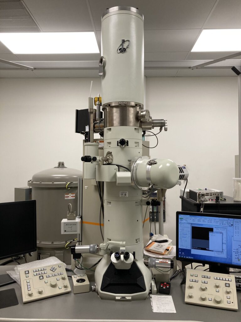
JEOL JEM-2100F Transmission Electron Microscope (TEM) (80-200 kV)
- Resolution: 0.195 nm TEM, 0.135 nm STEM
- Detectors: TEM (Gatan Rio CMOS), STEM (BF, ADF)
- Specimen Holders: Single-tilt, double-tilt, high-tilt (for tomography/microED), low-background EDS
- Analytical Tools: EDS (Oxford SSD, Aztec software)
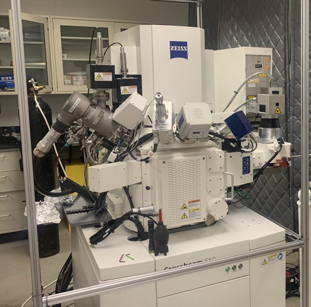
ZEISS Crossbeam 550 Laser FIB Scanning Electron Microscope (FIB-SEM)
- Tri-beam microscope integrating a field-emission SEM, focused ion beam (FIB), and femtosecond laser
- High-resolution imaging with Gemini SEM column
- Precision ion beam milling for site-specific cross-sectioning and sample modification
- Rapid bulk material removal with femtosecond laser while minimizing thermal damage
- TEM lamella preparation for high-resolution transmission electron microscopy
- Serial FIB-SEM sectioning and three-dimensional reconstruction
- Nanofabrication, failure analysis, and subsurface characterization
- Compatible with a wide range of materials, including metals, ceramics, semiconductors, polymers, batteries, geological samples, and biological tissues
EM Sample Preparation Tools
- Quorum Q150T ES Plus Coater: Metal sputtering and carbon evaporation for conductive coatings, with high vacuum capability and film thickness control.
- Pace Technologies PICO 155P Precision Cutter: High-accuracy wafering saw for sectioning metals, ceramics, and electronics (≤0.5 cm thick).
- Pace Technologies NANO 2000T Grinder-Polisher: Dual-wheel system for grinding and polishing various materials.
- Pace Technologies Giga-0900 Vibratory Polisher: Adjustable frequency polisher for simultaneous preparation of multiple samples.
- Plasma Cleaner: Removes hydrocarbons and modifies TEM substrates using oxygen or argon plasma.
- Bio-Rad Critical Point Dryer: Prepares delicate biological and other soft specimens for SEM by eliminating surface tension during drying. This process preserves specimen morphology and minimizes drying artifacts for high-quality SEM imaging.
- Reichert-Jung Ultracut E Ultramicrotomes: For cutting thick and ultrathin resin sections, on either glass or diamond knifes, for TEM or SEM.
- Leica EM TP Automated Tissue Processor: Programmable for automated fixation, staining, washing, dehydrating, and embedding EM samples with built in liquid handling, heating, cooling, and stirring.