The Electron Microscopy Lab is a research and service facility, serving the biological and materials research communities at CSU. It is open to university, state, and outside users. It houses one scanning electron microscope and two transmission electron microscopes to provide detailed imaging of surfaces, thin films, and nanostructures. Microstructural crystallographic analysis via electron diffraction and elemental analysis via energy dispersive spectroscopy are available.
The facility offers a wide range of services, including (1) imaging of thin films or nanoparticles at atomic resolution using the 2100F TEM and secondary electron imaging (SEI) and/or backscattered electron imaging (BSE) of surfaces at nm resolution in the SEM, (2) crystallographic analysis from thin samples using various modes of electron diffraction in the 2100F TEM and electron backscatter diffraction (EBSD) from bulk crystalline samples in the SEM, (3) spatially-resolved elemental analysis via energy dispersive spectroscopy (EDS) in the SEM and in the scanning transmission (STEM) mode in the JEOL 2100F TEM, (4) and e-beam lithography in the SEM.
Sample preparation tools include gold, chromium or carbon coating, sectioning and embedding soft matter and biological specimens, and a saw, grinder, and a variety of mechanical polishing wheels (for further information go to https://www.research.colostate.edu/iss/sample-preparation-tools/).
Instrument use and technician services are available on a recharge fee basis. Users can be trained in order to operate the microscopes by themselves. Alternatively, they can request assistance from the staff. User training on the 6500 SEM requires a few hours with a staff member and training on the 2100F TEM requires enrolling in an 8-week course with Dr. Roy Geiss.
Please use the iLab Portal to request training or services and access the instrument calendars.
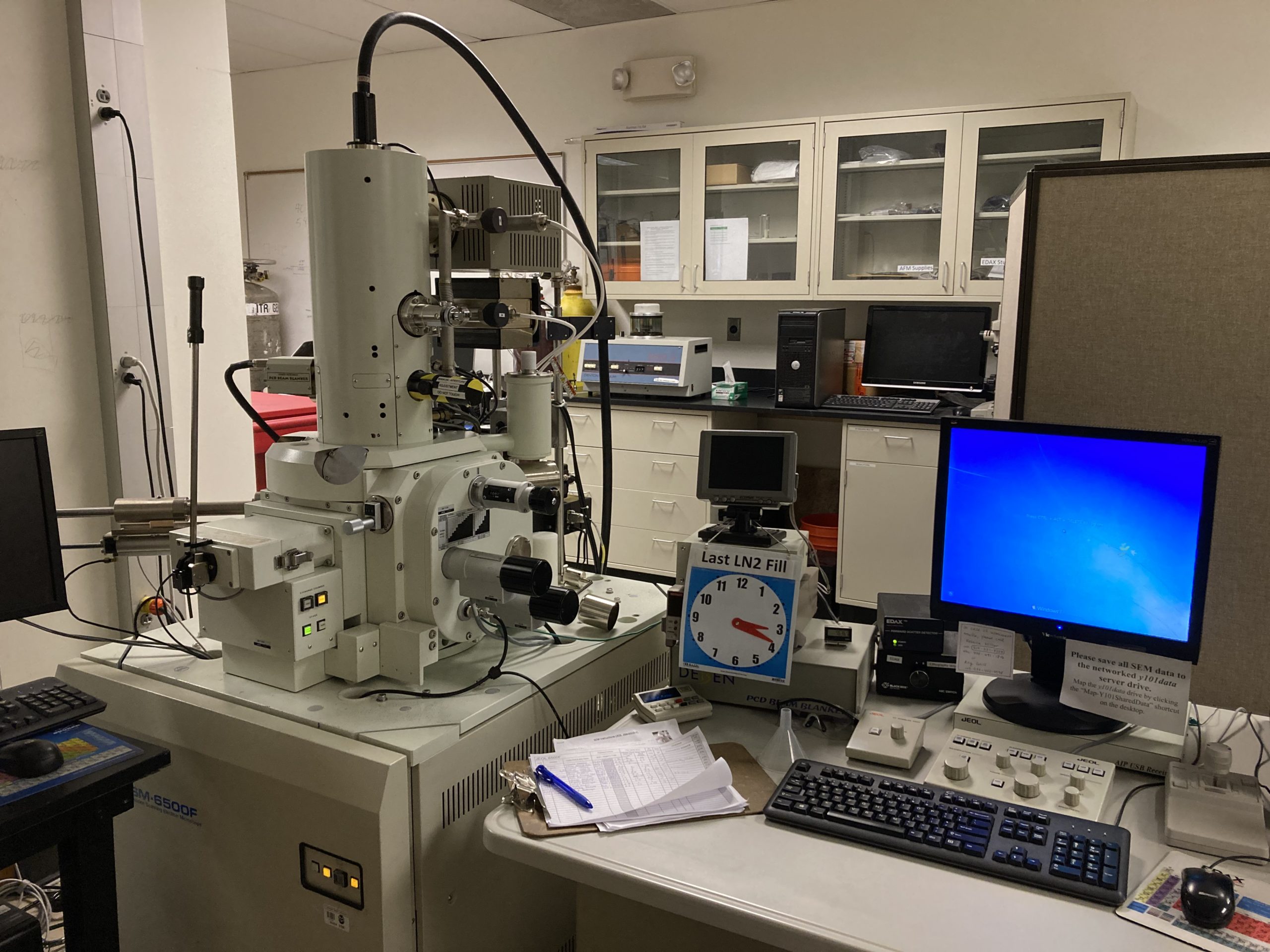
JEOL JSM-6500 Field Emission Scanning Electron Microscope
The SEM is equipped with the In-Lens thermal field emission electro gun (TFEG). This high-resolution tool has a multi-purpose specimen chamber and a motorized, automated stage. The SEM is equipped with an Oxford Instruments energy dispersive X-ray spectrometer (EDS) and uses Oxford Aztec software for qualitative and quantitative elemental analysis. It also has a Nabity e-beam lithography patterning system (NPGS). The NPGS allows for lithographic patterns to be written with our SEM a few tens of nanometers in width. There is a solid-state BSE detector for BS electron imaging, a special holder for STEM imaging of thin films and an EDAX EBSD camera for diffraction.
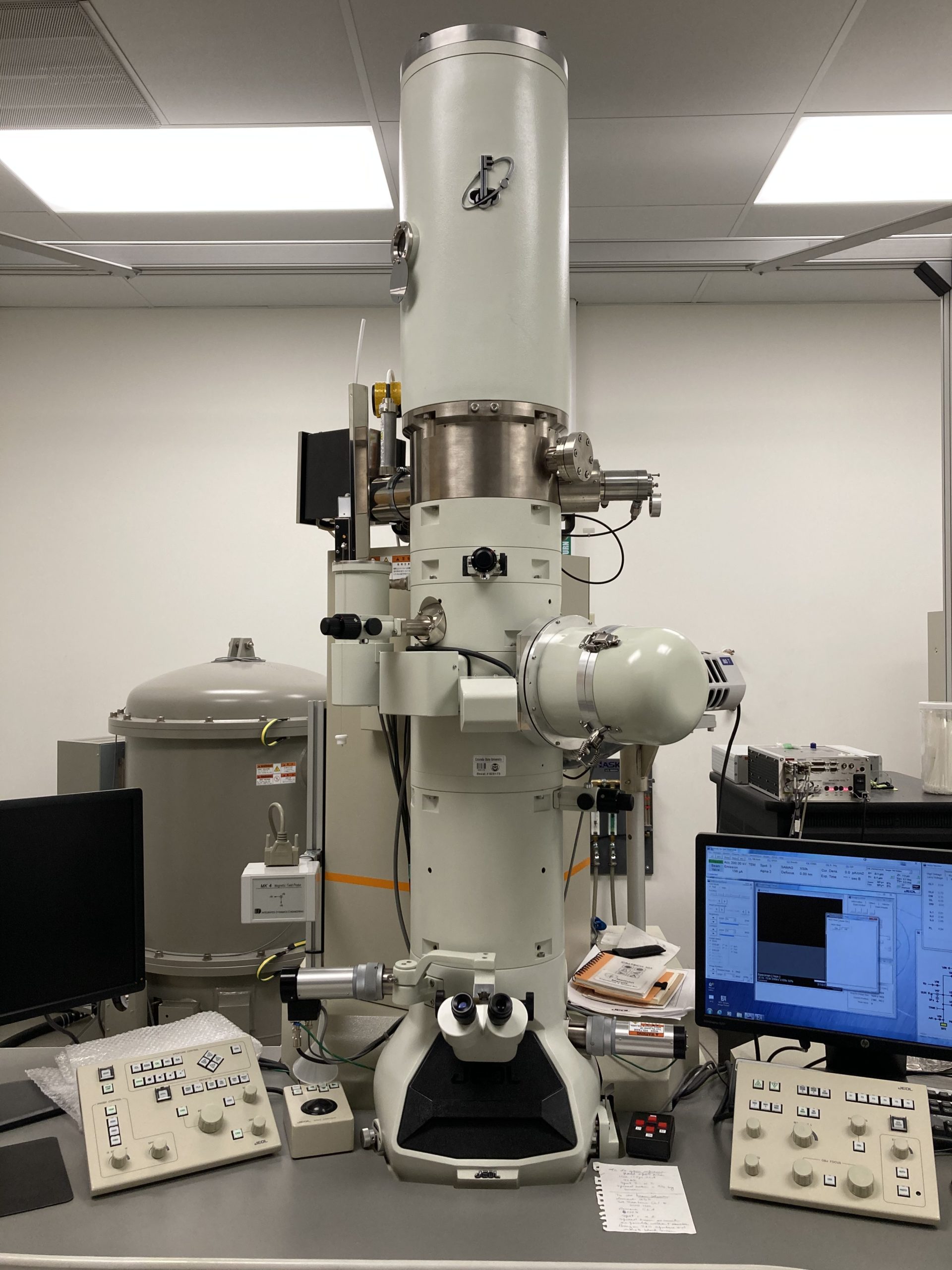
JEOL JEM-2100F Transmission Electron Microscope (80 – 200 kV)
The TEM is equipped with several specimen holders, including (1) a single-tilt holder with ± 20° tilt about the x-axis (rod axis), (2) a double-tilt holder with ± 20° tilt about both the x- and y-axes, (3) and a beryllium double-tilt holder with ± 20° tilt about both the x-axis and y-axes, specifically for low background EDS analysis. There is also a special high tilt holder that provides ± 40° about the x-axis using special samples and can be used for tomography and microED analysis.
This TEM has an UHR objective lens pole piece that provides 0.195 nm TEM image resolution and 0.135 nm STEM resolution. TEM images and diffraction patterns are captured with a Gatan Ultrascan 2K x 2K CCD camera. For STEM imaging there are three detectors: (1) a JEOL bright-field (BF) STEM detector, (2) a JEOL annular dark field (ADF) detector, and (3) a Gatan ADF detector. There is an Oxford Instruments SSD EDS detector with Aztec software for elemental analysis.
*User training on the TEM requires enrolling in an 8-week, extensive course with Dr. Roy Geiss.
Please see our Rates webpage for pricing information.
A Guide to Scanning Microscope Observation from JEOL
Williams & Carter: Transmission Electron Microscopy: A Textbook for Materials Science (textbook and online access available via CSU Library)
EDS in the TEM Explained from Oxford Instruments
Coming soon!